Page 1 of 2
NAND Flash Chips on D Series
Posted: Sun Oct 16, 2011 11:02 pm
by erdem_ua
Hi there. Since my board is bricked. I inspecting board more for revive it back.
Board belongs to UA40D6000.
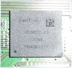
So I identified 2 flash chip at D series HW. One of them is SDIN502-2G Flash which is used in Amazon Kindle.
This chip used as main program storage, holds /dev/mmcblk0 device.
And other one is Samsungs Flash NAND chip, KFG1GN6W2D is used for /dev/stl0 device. This devices 12.th partition (/dev/stl/12) mounted as /mtd_rwarea.
I needed to change this chip content. Probbly by (un)soldering.
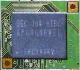
Decode: It's Samsung OneNAND (KF), Single chip (G), 1Gbit (1G), Technology (N), x16 Organization (6), ???Volt (W), 2KB Page architecture (2), Version d ? (D)
-HIB6 = Package format ? (H), Industrial Temp (I) , Include Bad Block product line (B), 66Mhz (6)
Re-programing this chips will solve the my bricked TV problem.
If you have any datasheet belong to those chips. I will be happy..
Re: NAND Flash Chips on D Series
Posted: Mon Oct 17, 2011 5:00 am
by juusso
Erdem, here is also stl0/13, which as you know is... mtd_exe...
Re: NAND Flash Chips on D Series
Posted: Mon Oct 17, 2011 9:55 pm
by erdem_ua
Then our only target is KFG1GN6W2D, since both start.sh and rc.local kept here.
Anyone know how could we handle this chips via JTAG.
Also heard that soldering BGA's is a problematic due old solders make noise. After removal chips balls became defected. They needed to be re-balled for re-install.
Re-Balling machines are too expensive. But I heard there is another cheap solution for that.
And also since this PCB's are lead-free, unsoldering the chips require more heat.
This heat also hazardous to chip. I think I let this soldering job to specialist

Before I needed to inspect what I could make via JTAG ports.
Re: NAND Flash Chips on D Series
Posted: Tue Jan 24, 2012 7:32 pm
by nobody
Why unsoldering?
If I recall correctly, there are TWO JTAG ports on the board!
By them you can read/write both flashes!
Re: NAND Flash Chips on D Series
Posted: Tue Jan 24, 2012 7:35 pm
by juusso
Yes? How to do that? Could you please be more detail.
What hardware is needed, what software, connection points and etc etc.
If you said A, please tell B
Re: NAND Flash Chips on D Series
Posted: Thu Jan 26, 2012 9:57 pm
by erdem_ua
Also, where is the second jtag port?
Re: NAND Flash Chips on D Series
Posted: Fri Jan 27, 2012 3:16 am
by nobody
erdem_ua wrote:Also, where is the second jtag port?
Maybe I'm wrong but I see 6 holes oooooo and next to them other 5 holes ooooo.
Also, the two connectors at the top of the board (sometimes the connectors are not soldered) should give the same functionality.

Re: NAND Flash Chips on D Series
Posted: Fri Jan 27, 2012 8:24 am
by sbav1
nobody wrote:
Maybe I'm wrong but I see 6 holes oooooo and next to them other 5 holes ooooo.
They look more like I2C EEPROM serial interfaces to me. Both of them. Probably no relation to JTAG and/or OneNAND flash whatsoever.
Picture is a little blurry; can you post pin description in text form?
Re: NAND Flash Chips on D Series
Posted: Fri Jan 27, 2012 10:56 am
by gooseye
Yep those are i2c for the serial eeprom located right by the pads. The jtag pads are up next to the socket for the CI adapter (on my D7000 mainboard that is).
Re: NAND Flash Chips on D Series
Posted: Fri Jan 27, 2012 5:33 pm
by nobody
sbav1 wrote:nobody wrote:
Maybe I'm wrong but I see 6 holes oooooo and next to them other 5 holes ooooo.
They look more like I2C EEPROM serial interfaces to me. Both of them. Probably no relation to JTAG and/or OneNAND flash whatsoever.
Picture is a little blurry; can you post pin description in text form?
Sorry.. I can't post better pictures, I made them in a hurry and I should open the tv to make new ones.
Yes.. they look like i2c bus to me, they have SDL SCL SDA lines labelled.
The jtag picture is also blurry but "almost readable":

Labels should be:
PLD_GND
PLD_TDO
PLD_TCK
PLD_TMS
PLD_TDI
unreadable